|
|
|
| Reference Series |
Table of Contents For This Issue
|
|
| |
| How Computers Work, Part I | |
|
August 2001• Vol.5 Issue 3 Page(s) 6-11 in print issue | |
Inside The PC's Brain How Microprocessor Circuitry Turns Electrical Pulses Into Computing Power You Can Use |
 A CPU gets its name because it is central to a computer’s operation in its role of either executing or controlling all data transfer and processing; it processes data and it is a single self-contained chip or unit. The CPU’s speed and performance are directly
related to a PC’s ability to do its work, making it by far the most vital of computer components.
A CPU gets its name because it is central to a computer’s operation in its role of either executing or controlling all data transfer and processing; it processes data and it is a single self-contained chip or unit. The CPU’s speed and performance are directly
related to a PC’s ability to do its work, making it by far the most vital of computer components.The question of how microprocessors do the things they do might never occur to some, and to others it might seem slightly akin to psychoanalyzing a genie that has just granted them three wishes. To be sure, the technology under a microprocessor’s hood is complex and highly sophisticated, but with an understanding of a few main components, figuring out how they work is easier than it would seem. Every instruction a microprocessor receives, whether programmed permanently into its instruction set or given to it as it processes an external and temporary set of instructions (software), is made up of commands that computer programmers have compiled into specific programming languages (for example, BASIC, COBOL, C, and others). In order to understand these commands, however, computers must first translate them into binary, a process that takes place within a microprocessor’s decode unit. For this to work, each letter of the alphabet and each base-ten number must be assigned a binary equivalent made up of ones and zeros. To this end, programs established different systems to form standard character sets that consist of letters and numbers translated into their binary equivalents. Systems such as EBCDIC(Extended Binary-Coded Decimal Interchange Code) and ASCII (American Standard Code for Information Interchange) give letters a numerical equivalent (for example, M equals 77 in ASCII), which is then translated into a binary form computers understand. So each time you press and hold the Shift key and the m key on your computer keyboard, it sends a signal to the computer’s processor which is translated internally from “M” into the binary equivalent of the number 77, or 01001101. In those terms, the letter is usable as pulses of electricity racing through a microprocessor’s various parts. Address. Numbers computers use to specify the location of a specific piece of data within memory or storage. CPUs often express data they are processing in terms of its address rather than its actual value. Bus. A set of conductor wires or conduits that transport data from place to place. A computer’s bus is the data or system bus, which sends and receives data to and from input/output devices, a system’s main memory, and its CPU. CPUs also have internal buses that carry data among units within the chip’s logic structure and address buses that connect them to a computer’s main memory. The computing industry classifies buses in terms of bit-width, or the number of bits of data that can travel through them simultaneously. In some cases, a processor’s internal bus is twice as fast as the bus that connects it to the rest of a computer’s components, as processors execute instructions at much higher rates of speed. For example, a PC might have a 32-bit system bus and a processor with a 64-bit internal bus.
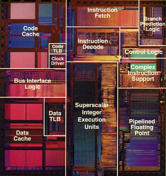
Clock frequency or speed. One of the major differentiations between various CPUs, clock speed refers to the number of cycles a CPU performs in the span of a tick of a computer’s internal clock, a crystal that resides on a computer’s motherboard and vibrates many times per second at regular intervals. The industry expresses clock speeds in terms of MHz, or millions of cycles per second. At press time Intel Pentium 4 processors, for example, come in clock speeds from 1.4GHz (or 1400MHz) to 1.7GHz (1700MHz). CPU clock speeds can be a bit misleading, as different computers may have faster or slower clock crystals and as different internal structures and instruction sets cause processors to perform at varying levels. As such, two different brands or models of processors with similar clock speeds often perform at different levels. Logic gate. A circuit made up of a series of transistors that perform Boolean logic operations (logical designation of either “true” or “false” based on the comparison of an on or off signal to the desired state) in order to implement computer instructions. RAM. A microprocessor takes software instructions from magnetic or optical storage sources, such as ROMhard drives, and CD-ROM drives, and places them in a computer’s main memory, or RAM, where they await access to its CPU. Although a computer’s RAM is not part of its CPU, the amount of RAM in a computer profoundly affects overall performance. Registers. Several small pockets of memory that store data internally while a microprocessor needs it. Because each register is very small, the number of bits the CPU uses to express the address of a desired piece of data within is very small. This makes registers much faster to access than normal memory, which can require as many as 20 bits of information just to specify an address. Transistors. Bell Labs’ 1947 invention of the transistor made microprocessors as we know them today possible. A transistor is basically a three-way junction in a processor’s circuitry and includes adjacent layers of negatively and positively charged material that either amplify an electronic pulse (allowing it to move on to the next transistor) or impede it. ALU(arithmetic logic unit). The portion of a CPU where mathematical operations and Boolean logic operations occur. Boolean operations are the logical comparison of binary values that determine whether an electronic pulse should be sent through a specific gate in a processor’s circuitry. These operations follow the basic format of “If x is true and y is false, then z is true.” Control unit. This performs one of four basic tasks for each instruction that a CPU receives from its instruction set (see below) or from user input. The tasks it performs are: •fetch—sending the address of the next word in an instruction to be executed on the address bus and placing the word in the proper location of the instruction cache •decode—sending the current instructions from the instruction cache to the decode unit •execute—initiating the processing of math and logic calculations within the CPU’s ALU and generally controlling the flow of data to their proper destinations •store—recording the result of the instruction in the proper register or memory location Decode unit. Also known as the instruction decoder, this portion of the CPU takes machine language instructions from the instruction cache and translates them into binary code so that the ALU can process them. FPU(floating-point unit). Some computer operations call for mathematical operations to be performed on non-integers (fractions expressed with decimals), which most ALUs can’t calculate. As a result, prior to 1989, chip makers added an external FPU chip to a computer’s motherboard to handle these more complex operations. Intel’s 80486 (usually known as the 486) was the first processor to incorporate an on-board FPU, and most chips since that time follow suit. Floating-point math operations most often occur when a PC is running software that produces high-end graphics, such as CAD(computer-aided design) software or games with 3-D graphics. Instruction set. A collection of machine language instructions stored permanently within the structure of a processor. The chip is designed to understand and execute the instructions based on its physical structure and permanent software coding. A chip’s instruction set tells it how to interpret and execute various tasks it must perform in order to run computer software. The two main types of instruction sets are CISC (Complex Instruction Set Computer) instructions and RISC(Reduced Instruction Set Computer) instructions. As its name implies, a RISC processor recognizes and executes fewer commands, which produces faster performance in most cases. Additionally, all RISC instructions are a set number of bits in length making them easier to process quickly, as opposed to CISC instructions, which may be from 8 to 120 bits in length. Intel x86 chips (from the Intel 8086 CPUs to the latest Pentium 4s) all use a CISC instruction set. Prefetch unit. A small amount of memory that stores incoming instructions in an electronic queue while awaiting execution. The prefetch unit checks the CPU’s instruction cache and main memory for further instructions about what to do with incoming instructions and determines the proper way to proceed while the decode unit and control unit decode and execute previous instructions. This reduces the time a CPU must spend waiting for instructions. For example, let’s walk through what happens when you access your specific user profile from within Windows Me at startup. As your computer comes to life, it initiates the WinMe startup as instructed by its instruction set and internal Windows commands. As it runs through the list of startup procedures, it encounters a set of commands that tell it to prompt the user for a User name and Password before providing access to any specific user profile settings. A dialog box appears, asks you for the specific information, and awaits your reply with a flashing cursor. (If only one User Profile is present, that name will appear in the User name field by default; otherwise the name of the most recent user to log on will appear). If your password is “Mozart,” for example, you would type it in the Password field and either click OK or press the ENTER key. Keystrokes. When you press the M key, the data bus sends this data through your PC’s main memory to its processor. Because the CPU’s instruction cache has no specific instructions about how to use the data yet, the keystroke data joins the line of pending instructions stored in the prefetch unit. The prefetch unit checks main memory for further orders (placed there by Windows or other software the computer is running), and the main memory instructs the prefetch unit via the data bus to send the data to the instruction cache, which assigns it a specific address for use in its retrieval. The prefetch unit gets the data’s address from the instruction cache and forwards it and the data to the decode unit. The decode unit translates the data (the letter M), the instruction that accompanies it, and its address in the instruction cache from machine code into binary as mentioned earlier and sends this information off to yet another digital destination, the control unit. The control unit reads the instruction from the decode unit, which tells it to store the data in the data cache, where it will stay until further instructions arrive. At this point the letter M is stored in your CPU’s data cache and its instruction cache at a corresponding address and appears on your monitor via your system’s data bus. All of the steps required to accomplish this task take place in the merest fraction of a second, and the letter M appears on-screen as the first letter in the Password field almost instantaneously as you press the key. Your CPU repeats this process for each remaining keystroke until all six letters of the word “Mozart” appear on your monitor and are stored in your CPU’s data cache and instruction cache. When you click OK or press the Enter key on your PC’s keyboard, a whole new process begins. Logic takes over. As you click OK, the command runs from your PC’s input controller through its data bus, into the prefetch unit. The prefetch unit checks the instruction cache for instructions, and when it finds none, it checks the main memory. The main memory, thanks to instructions put there by Win98, sends the prefetch unit a set of values (“Mozart”) and instructs it to send the new data to the instruction cache with instructions to compile the previous input and compare it to the new data. The prefetch unit sends these instructions to the instruction cache and retrieves the resulting data addresses, which it passes on to the decode unit. The decode unit translates all of the data and instructions from machine code into binary code and sends them onto the control unit. The control unit reads the binary code instructions, including the data to compare your input to, and sends a sequence of logic operations to the ALU for processing. The control unit sends the first letter of the password received from WinMe to the ALU in its binary form. The control unit also sends the addresses of the first piece of your input (the letter M), which, as you will recall, is stored in data cache. The ALU then proceeds to run a series of Boolean logic operations to compare the values of each binary digit in your input to those provided by WinMe. As the ALU checks each 1 and 0, they match up, and the ALU goes on to the next, until it verifies each binary digit that makes up the letter M. The ALU then stores the results of its operations (“true” or “false”) in a memory register and goes on to look at the next letter of the password. This process repeats until all six letters are checked. The ALU finishes its job by storing the results of each comparison in a register. In the meantime, the main memory has instructed the control unit by way of the prefetch unit, the instruction cache, and the decode unit to launch Win98 with full access to your User Profile if the ALU responds “true” upon comparing each value in the password for a match. If you typed your password correctly, the control unit prompts the prefetch unit to obtain instructions for opening Win98 from the main memory.
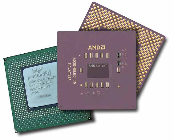
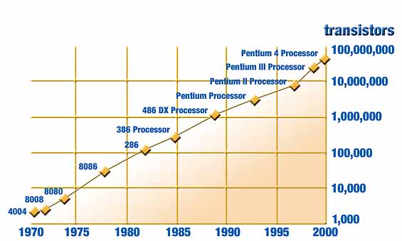
Since then both general computing technology and microprocessors specifically have advanced at a steady pace. Intel’s latest consumer offering is the Pentium 4 (codenamed Willamette) processor, which currently reaches clock speeds of 1.7GHz. This speedy chip contains 42 million transistors connected by aluminum wires .18 microns wide and comes integrated with 256KB of secondary, or L2 cache memory. AMD (AdvancedMicro Devices) is another prominent PC microprocessor manufacturer that uses its Athlon processor with 3DNow! technology to compete withIntel. June 2001 saw AMD debut the Athlon 4 (codenamed Palomino); the Athlon 4 contains roughly 37.5 million transistors and has 128KB of L1 cache and 256KB L2 cache. Intel recently announced that 20 nanometer transistors will enter production as the building block for their 45 nanometer process generation due in 2007. One nanometer is one-billionth of a meter and 20 nanometer transistors are 30% smaller and run 25% faster than today's fastest transistors. Smaller transistors translate to speed. And speed is the goal of advancing microprocessor technology. This year CPUs will hit 2GHz, but 2007 should see CPUs coming up on speeds of 20GHz. The IBM PowerPC line of microprocessors includes the PowerPC 750, a chip that comes in clock speeds of up to 500MHz, contains 6.35 million transistors, features 64KB L1 cache, and can support three sizes of L2 cache up to 1 MB. The PowerPC 750’s most interesting feature is its use of copper pathways to transport signals throughout the chip rather than the older aluminum technology. (See Building The Perfect Processor for more information on the materials used in making microprocessors.) Copper is a much better electrical conductor than aluminum, and as the technology to manufacture copper-wired processors becomes more practical to implement, you can expect several companies to follow IBM’s lead.
We spoke at length with Intel spokesman Howard High about Moore’s Law and the current performance of high-end microprocessor chips: “Typically, over time, you'll see roughly a doubling. Like when we went from .25 to .18 on Pentium III, we had kind of peaked out on .25 micron in the range of 600MHz. We went to Coppermine starting at 600 and we're at 1GHz on the Pentium III and 1.7GHz on the Pentium 4. We'll have 2GHz [.13 micron copper CPU codenamed Northwood] fairly soon on P4, and when you take to .13 and [start] the P4 at 2GHz, over time I think you can expect that frequency to probably double again.” In short, this means that while today’s CPUs are incredibly fast, we can expect the magic that goes on within their amazing, microscopic networks of transistors and wires to continue getting faster. by Chris Trumble View the graphics that accompany this article. (NOTE: These pages are PDF (Portable Document Format) files. You will need Adobe Acrobat Reader to view these pages. Download Adobe Acrobat Reader)
| |||||||||||||||||||||||||||||||||||