|
|
|
| Reference Series |
Table of Contents For This Issue
|
|
| |
| How Computers Work, Part I | |
|
August 2001• Vol.5 Issue 3 Page(s) 120-125 in print issue | |
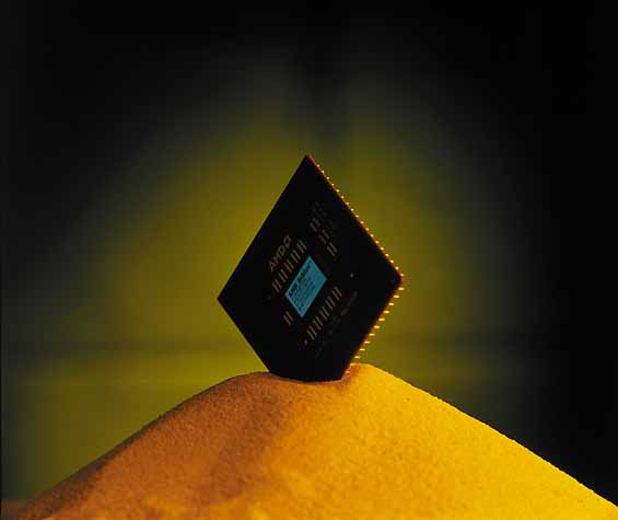
Building The Perfect Processor Demystifying The Microprocessor Construction Process |
These instructions travel in the form of electronic pulses through a network of tiny, aluminum wires that are less than 1/100,000th of an inch wide (0.18 microns, to be exact). These millions of transistors and all of these aluminum wire pathways fit within a silicon wafer, 217 square millimeters in area, that attaches to your PC’s motherboard with 423 (or, in some cases, 478) metal pins. If you’re like most computer users, you spend little time worrying about how manufacturers pack all that stuff into such a small, plastic and silicon case. You just know that when you push the power button, the PC comes alive and makes your life easier. But the amazingly complex processes that take place at companies such as Intel and Advanced Micro Devices during the creation of these tiny, silicon “brains” are quite fascinating. Making microprocessor chips requires exacting, no-compromise engineering and cleanliness; designing them takes a healthy research and development budget and a full stable of geniuses. Once designers define the tasks a microprocessor should be able to perform and the instructions it should use (the built-in software that makes a chip run, such as RISC [Reduced Instruction Set Computer] or CISC [Complex Instruction Set Computer]), they can map out the network of wires and transistors that make up the chip’s logic architecture. This painstaking process requires a sizable team of engineers working for months or even years. Extensive planning, diagramming, and revision ensure that when a chip finally goes into its production phase it will work correctly. Using computer modeling and design prototypes, engineers evaluate the effectiveness of their designs and find any flaws. Then they take the information and go back to the drawing board to refine a chip’s design, test some more, and so on, until they can be certain a chip will function properly. In addition to designing a chip’s internal structure, engineers must take great care in choosing the materials and processes used in the microprocessor’s construction. We’ll talk more about up-and-coming developments in these areas later, but for now there are a few basic materials and steps that nearly everybody in the microprocessor industry uses. Silicon. Two key qualities of silicon make it attractive to chip builders. First, it trails only oxygen on the list of nature’s most abundant elements (ever heard of a sand shortage?), making it inexpensive. Second, silicon is one of nature’s best electrical conductors. It is also fairly simple to alter silicon’s properties where necessary to prohibit electrical conductivity, making it the perfect semiconductor (a material that can act either as a conductor or insulator).
Aluminum & copper. Today’s microprocessors consist of several million transistors, all connected by a network of pathways capable of carrying electrical impulse signals from place to place. These pathways are minuscule wires made of metals that conduct electricity efficiently, most commonly aluminum and copper. Copper is the better electrical conductor, but many microprocessor companies continue to use aluminum because copper and silicon contaminate each other when they come into direct contact. This creates the need for a microscopic barrier between the two wherever they meet, which adds an additional step to the manufacturing process. IBM has led the industry in bringing copper wires into the chip-making process on a large scale, but Intel and other companies are currently making plans to incorporate copper into their chips in the near future as the processes used to create the necessary barriers become more viable. Chemicals, gases & light. In order to produce microprocessors efficiently on a large scale, companies use a wide variety of chemicals and gases to accomplish several types of tasks. These items range from complex gases such as hexa-methyldisilazane (try saying that five times really fast) to simple elements such as boron. Exposure to certain gases creates thin barriers of silicon dioxide that prohibit conductivity across a silicon wafer’s surface, and chemical solutions wash away the silicon dioxide as prescribed by a chip’s design specifications. Low-frequency light waves are also integral to the construction process in their role of placing the desired circuit pattern on a microprocessor with the help of an ultra-thin layer of light-sensitive material known as photoresist. Much like normal light re-creates images and colors when it shines on the film used in cameras, certain ultraviolet lights invisible to the human eye create the image of a circuit pattern in photoresist, which yet another chemical process places on microprocessors.
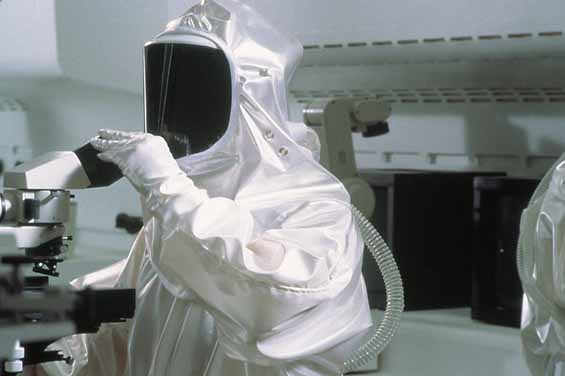
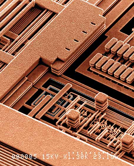
A speck of dust inside a processor, although only the relative size of a soccer ball in the entire country of Ireland, is large enough to cause problems. Thus the “bunny suits” worn by dancers in Intel commercials symbolize more than just corporate mascots or colorful characters. Employees at Intel and other microchip manufacturers wear bunny suits during microchip fabrication to protect the delicate chips from contamination by even the tiniest bits of dust, hair, or skin that we all leave behind as we move and touch things around us. But these suits are only the beginning. Microchip manufacturing occurs in areas called “clean rooms” that let companies tightly control and monitor every environmental element. High-tech filtration systems constantly circulate the air in clean rooms to remove every particle of dust and debris, completely replacing a clean room’s air about 10 times per minute. Other systems control all of the chemicals, gases, and water used at various steps of fabricating, filtering, controlling, and closely monitoring them for purity and cleanliness. Before entering a clean room, technicians follow a painstaking process to ensure that no particulate matter or contaminant enter the ultra-clean environment with them. All personal items, except for a few that are approved, must remain in a storage area. Workers remove makeup, cover head and facial hair with lint-free covers, and individually clean shoes and any items taken into the clean room. This done, Intel employees must sit on one side of a bench that is divided into specially designated “dirty” and “clean” sections, place a bootie over one shoe, swing that foot over to the clean side of the bench, and repeat the process with the other foot. Then workers enter another room in which they don gloves and the rest of their bunny suits, attach a personal air filtration system and battery pack to the belts of their suits, and put on a helmet, safety glasses, and disposable face shield. Only then are they allowed to venture into a clean room’s confines. A chip’s surface and the amazingly small network of circuitry visible on it seem impressive enough, but in reality there is much more to these chips. Today’s microprocessor comprises approximately 20 micro-thin layers of such technology, each one stacked upon the others. The ground floor. Chip makers divide the aforementioned 8-inch wafers into many square units that will each become the base of a microprocessor (sometimes numbering in the hundreds, depending on the chip size). Then they expose the wafer’s surface to extreme heat and special gases, which promote the growth of a thin layer of silicon dioxide. Intel likens the growth of silicon dioxide on silicon to that of rust on metal, except that the processes used cause it to develop much faster. This silicon “rust” ensures that the electricity that will eventually run through the chip’s circuitry does not conduct through the entire chip. With a layer of silicon dioxide in place, the wafer undergoes a chemical process that creates a layer of photoresist (mentioned above), which will host the pattern of the first layer of the chip’s circuitry. Photolithography. A microprocessor chip’s transistors and the wires that connect them are extremely small. Most of today’s manufacturers currently use pathways that are a mere 0.18 microns (a micron is one millionth of a meter, or approximately 1/25,000th of an inch) wide. Companies use a process called photolithography to create spaces this minute on a silicon wafer’s surface. Engineers create a mask, or stencil of sorts, that bears an exact image of the circuitry pattern to be placed on the chip. They place this mask over the wafer and subject the wafer to extremely low-frequency ultraviolet light. The mask allows for the circuitry pattern to shine through and hit the wafer, while protecting the rest of the wafer surface at the same time. The UV light hits the thin layer of photoresist covering the wafer, changing its consistency and letting a chemical solvent dissolve the affected area. Once the photoresist dissolves and washes away, the pattern remaining on the wafer’s surface exposes the silicon dioxide beneath, which is in turn etched away by more chemicals to expose the pure silicon in the desired pattern. Chemical solvents then remove the remainder of the photoresist layer, leaving the circuit pattern etched into the original pure silicon base of the wafer in the form of 0.18-micron pathways between ridges of silicon dioxide. Building a silicon high-rise. Once the initial circuitry pattern is in place on the silicon base, Intel and other companies grow another ultra-thin layer of silicon dioxide across the top to act as a barrier between the first and second layers. Technicians create the second level upon a much thinner layer of silicon than the original wafer, but use the same lithography procedure with a different mask or pattern stencil. The new mask includes its own circuitry pathways, as well as numerous junctions with the layer below.
As the process adds more layers, the “wires,” or metal strips that fill the circuitry pathways and connect the transistors between each level, arrive through the deposits of atoms of metal (usually aluminum) on to the wafer’s surface, filling the pathways and junctions that exist between each level. These steps repeat until the wafer has the desired number of layers, which often requires a sequence of more than 250 steps. Once completed, these processes create several complete microprocessors per silicon wafer, each of which is tested to determine the integrity of its circuitry and transistors. This done, a computer-controlled, high-precision diamond saw divides the wafer into individual chips. Shell ‘em & ship ‘em. Once the microprocessor’s internal structure is complete, it is time to encase it in a plastic shell. Some chips need only a protective black plastic cover with connectors that will attach them to PC motherboards or other specialized types of circuits, depending on its intended use. Others, such as Intel’s Pentium III processors, get large plastic cartridges that also contain small amounts of cache memory (ultra-fast memory used to store instructions waiting to be processed). After this step, computers run tests on each microchip a final time to ensure everything works before manufacturers package them. Intel continued its aggressive research in microprocessor technology, and the 200KHz 8008 made its debut in 1972. It contained 3,500 transistors and was twice as powerful as its predecessor. This gave way in 1974 to the 8080, which contained 6,000 transistors and pathways just 6 microns wide. (Narrower pathways allow for faster clock speeds, because they offer less resistance to pulses traveling through them, which in turn creates less heat.) The 8080’s most famous use was in an early microcomputer called the Altair, which was the first commercially successful personal computer, selling through mail order for about $395. The Altair’s manufacturer, MITS (Micro Instrumentation and Telemetry Systems), began shipping its computer with a computer language program called Altair BASIC (Beginner’s All-purpose Symbolic Instruction Code, originally written in the mid-1960s). Bill Gates and Paul Allen, who would go on to form Microsoft, developed Altair BASIC in 1975. The last 20 years. In 1978 Intel introduced its next microprocessors, the 8086 (5-10MHz) and 8088 (5-8MHz). These processors consisted of 29,000 transistors and electronic pathways 3 microns wide. IBM chose the 8088 to be the brains of its highly successful IBM PC. Intel forged ahead throughout the 1980s, developing its 80286 (6-12.5MHz, 134,000 transistors, 1.5-micron pathways), 80386 (16-33MHz, 275,000 transistors, 1-micron pathways), and 80486 (25-50MHz, 1.2 million transistors, 0.8-micron pathways) processors. By this time, a number of computer manufacturers sold clones, replicas of IBM’s PC, fueling steady growth in the microprocessor market. Intel’s technological development kept pace, leading to the introduction of the first Pentium processor in 1993. The Pentium, or 80586, continued to use 0.8-micron pathways but integrated a staggering 3.1 million transistors on a single silicon microprocessor chip. The Pentium and Pentium MMX chips came with clock speeds of 60MHz up to 266MHz and were the first to integrate superscalar architecture, the ability to execute more than one instruction per clock cycle (a 200MHz processor executes 200 million clock cycles per second). Additionally, the first Pentiums came with a bus width of 64 bits, twice that of the 80486 chip. A processor’s bus width determines how many bits of information the CPU’s data bus can transfer to and from the processor at one time. These improvements represented significant leaps in performance and helped take personal computing to new heights. Today & tomorrow. Intel continues to push the envelope in microprocessor technology today, having crashed through the 1,000MHz (or 1GHz) barrier last year with the release of its Pentium 4 processor. This follow-up to its Pentium II (200-466MHz, 7.5 million transistors, 0.25-micron pathways) and Pentium III (450-600MHz, 9.5 million transistors, 0.25-micron pathways) processors contains 42 million transistors, or more than four times the amount of its immediate predecessor, and uses 0.18-micron pathways. According to Intel Spokesman Howard High, the company has no plans of slowing down. High says 0.13-micron technology should be in PCs and on retail shelves sometime during the third quarter of 2001, and that the new process should lead to clock speeds in the 4-5GHz range as early as next year. “I’ve been in the business 20 years, and this is the part that I still think at the end of the day is black magic,” High says. Not to be outdone, AMD has developed its own line of 1-1.4GHz Athlon processors and has made considerable strides in the high-end desktop PC market of late. Of course, in order to make these continuing leaps in speed and miniaturization, engineers must constantly evaluate new materials and construction processes to determine their feasibility. More and more companies will soon follow IBM’s lead in the use of copper rather than aluminum in constructing the circuitry pathways, due to its increased conductivity. High says that all of Intel’s processors, starting with the switch to 0.13-micron technology, will include copper metalization. Another change on the horizon is Intel’s growth and utilization of silicon crystals that are 12 inches in diameter, rather than 8 inches. The company can manufacture many more microprocessor chips on a 12-inch wafer of silicon than on the current 8-inch wafers for about the same cost. High says Intel will likely switch to 12-inch wafers early next year and that other companies will likely follow suit at some point to avoid a cost/margin disadvantage. The good news for consumers is that such a change is likely to continue to drive CPU costs down. The most significant technological advances, however, should come in the area of photolithography. The light source Intel uses today is a deep ultraviolet light with a wavelength that is just 193 nanometers (a micron equals 1,000 nanometers) wide. Manufacturers can use this same light source to make 0.13-micron pathways, but making them much smaller will require new light sources with even narrower wavelengths. Intel and other companies are currently working on a 157-nanometer light source that will let them create 0.10-micron pathways and another light source just 13 nanometers wide. The obvious question is whether there is a limit to how small microprocessor circuitry pathways can be made. “There is a particular point in time when we’ll get down to where the line that we’re trying to etch is smaller than the spaces between the atom that we’re trying to etch it on, so that does create certain changes in our approach, but we’re not there yet,” High says. by Chris Trumble View the graphics that accompany this article. Processor Progress How Microprocessors Are Manufactured (NOTE: These pages are PDF (Portable Document Format) files. You will need Adobe Acrobat Reader to view these pages. Download Adobe Acrobat Reader)
|